Complete Guide to CoWoS Process: The Key Advanced Packaging Technology for the AI Era
- Amiee

- Apr 16
- 3 min read
Updated: Apr 17
As AI, high-performance computing (HPC), autonomous vehicles, and data centers evolve rapidly, traditional semiconductor packaging methods struggle to meet increasing bandwidth and integration demands. CoWoS (Chip-on-Wafer-on-Substrate), developed by TSMC, emerges as a vital solution, driving the future of multi-die integration and advanced packaging platforms.
In this article, we provide a comprehensive walkthrough of CoWoS technology, from its process flow and key architectural elements to real-world use cases and future roadmap.
What is CoWoS?
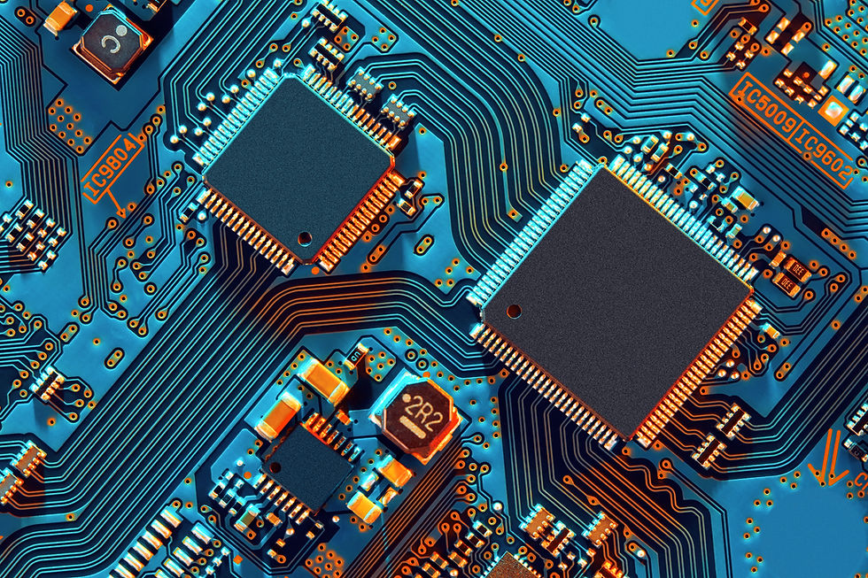
CoWoS, short for Chip-on-Wafer-on-Substrate, is an advanced 2.5D packaging technology pioneered by TSMC. Unlike traditional SoC integration, CoWoS enables heterogeneous integration by combining multiple dies—such as SoCs, GPUs, and HBM memory stacks—on a silicon interposer, which is then bonded to a substrate.
The silicon interposer features high-density metal interconnects and TSVs (Through-Silicon Vias), providing ultra-high-bandwidth, low-latency data communication between chips. This results in improved power efficiency, thermal performance, and compact footprint—critical for next-gen AI, HPC, and cloud workloads.
Background and Evolution
As Moore’s Law slows, and transistor scaling hits physical and economic limits, the semiconductor industry turns to advanced packaging to maintain performance growth. Since its launch in 2012, CoWoS has evolved to support various architectures:
CoWoS-S (using large silicon interposers)
CoWoS-R (RDL-based interposers with organic materials)
CoWoS-L (modular integration with local silicon interconnects)
CoWoS enables chiplet-based design, improves memory bandwidth, and meets the demands of workloads like AI training, inference, 5G, and data center acceleration.
Core Architectural Elements
Silicon Interposer
Provides short, high-speed signal paths and supports multiple large dies and up to 8 HBM stacks. Enables tight die-to-die integration with excellent signal integrity and thermal performance.
Redistribution Layers (RDL)
Key to CoWoS-R and CoWoS-L variants, RDL enables flexible I/O routing and efficient use of substrate area. CoWoS-R uses organic substrates, while CoWoS-L incorporates modular LSI bridges for larger system configurations.
Die Stacking and Integration
Supports multiple chiplets and HBM memory. Enables customized die mix-and-match integration, reducing latency and power while enhancing performance.
CoWoS Process Overview
CoWoS manufacturing involves a high-precision multi-stage process:
Die Preparation & Bonding
Known Good Dies (KGD) are cleaned and pre-processed before bonding. Micro-bumps, typically tens of microns in diameter, are used to electrically and mechanically bond each die onto the silicon interposer. High-precision alignment and thermal control ensure interconnect reliability.
Interposer Assembly
The interposer incorporates Redistribution Layers (RDL) and TSVs. RDLs are metal-insulator layers that fan out I/O connections to the right positions. TSVs provide vertical signal paths through the silicon interposer, connecting the dies to the package substrate.
After bonding, reflow and initial electrical tests verify the integrity of micro-bump connections.
Substrate Attachment & Final Assembly
The die-interposer stack is attached to an organic substrate using solder balls. Underfill resin is applied to strengthen thermal-mechanical stability. Heat spreaders or lids are added for thermal dissipation. Final testing includes electrical, signal integrity, and reliability validation.
The result is a compact, high-performance multi-die module ready for AI and HPC deployment.

CoWoS in Real-World Applications
AI and Machine Learning
NVIDIA’s H100 (Hopper) adopts CoWoS-S with 6 HBM3 stacks to achieve over 3 TB/s of bandwidth. The newer Blackwell B100/GB200 chips use CoWoS-L with 12 HBM3E stacks, pushing memory bandwidth and thermal design boundaries.
High-Performance Computing (HPC)
Used in exascale systems like ORNL’s Frontier supercomputer, CoWoS integrates logic dies and HBM in a thermally efficient layout, enabling extreme parallel computing for physics, simulation, and AI models.
Networking and Telecom
CoWoS-R enables cost-effective integration of SoC, switch fabric, and high-speed PHYs for routers, switches, and 5G base stations using RDL interposers and organic materials.
Future Outlook for CoWoS (Verified)
TSMC’s roadmap shows continued scaling of interposer sizes (beyond 3.3X reticle) and HBM support (up to 12+ HBM4). CoWoS-L introduces modular design and higher yield, enabling massive chiplet-based systems.
Hybrid architectures like active interposers, bridge interposers, and system-in-package (SiP) integrations will further expand CoWoS’s role. CoWoS is evolving from a packaging solution to a system-level enabler.
Conclusion: Building the Future, One Layer at a Time
CoWoS is no longer just a niche packaging solution—it’s a foundational technology shaping the future of AI and HPC infrastructure. From HBM stacking to silicon bridges, it enables data to flow faster, cooler, and smarter.
So next time your AI model finishes training just a little too quickly, don’t forget to thank that quiet little CoWoS module—it probably rerouted time itself. 😉